Demcon high-tech systems logo diapositive
  • markets
    • Semicon
    • Quantum technology
    • photonics
    • Analytical & Measurement systems
    • Energy transition
    • Big science
    • Aerospace
    • Food & Agri
  • services
  • expertise
  • tech insights
  • about us
    • Locations
  • Contact
  • careers
  • news
  • events
header thermal drift showcase
  1. Home›
  2. Tech insights›
  3. Thermal drift in precision engineering

thermal drift in precision engineering.

This article showcases the expertise of Demcon multiphysics and was originally published in Mikroniek, issue 6- 2024, pp. 16-19.

The phenomenon of thermal drift compromises precision as a result of thermal expansion or contraction of components, caused by small variations in temperature. Various mitigation strategies exist to minimise the effect of thermal drift on precision. Through modelling of thermal systems, the magnitude of thermal drift and the effectiveness of mitigation strategies can be predicted, using for example the lumped-element method (LEM) or the finite-element method (FEM).

introduction

Thermal drift is caused by small variations in temperature that lead to thermal expansion or contraction of system components as a result of internal or external heat sources, which can cause small offsets in position/distance measurements.

Fluctuations in ambient temperature and heat dissipation by actuators or sensors depending on load cycles are unavoidable to a certain extent and cause thermal drift in a system. Thermal drift is typically slow to stabilise or will never fully stabilise, as temperature is difficult to control precisely and it can take a long time for a system to reach a thermal steady state. Multiple strategies exist for handling thermal drift to mitigate its effect on precision.

The use of materials with a low coefficient of thermal expansion (CTE), like Invar or Zerodur", is a common strategy in precision engineering to minimise the effects of thermal drift.

However, also the thermal diffusivity (the thermal conductivity divided by the mass density and specific heat capacity) of a material is an important property to consider. A low thermal diffusivity often leads to uneven temperature distributions in components, which cause bending or warping deformations that are often more problematic than uniform thermal expansion.

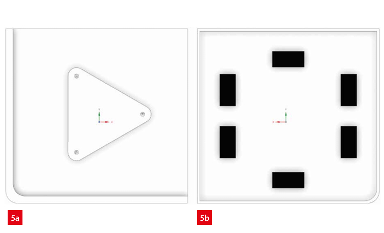
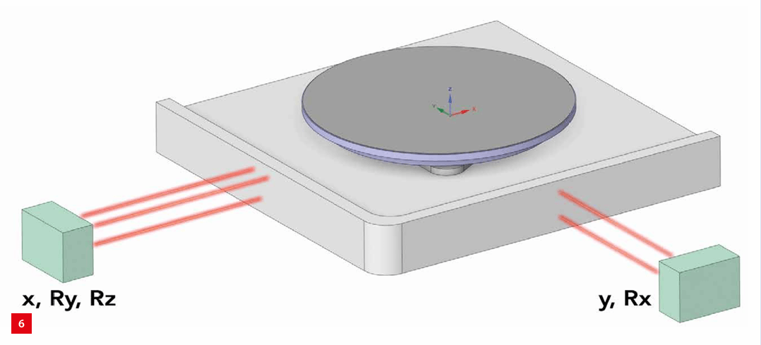
In some instances, the effects of thermal drift can be eliminated by identifying the thermal centre of a component: when a component is constrained in a statically determined manner, a thermal centre exists that does not displace under homogeneous thermal expansion of the component. When two components have their thermal centres aligned, temperature variations will not lead to misalignment.

Heat transfer is thermal energy in transit due to a spatial temperature difference. Thermal drift of critical components can be minimised by, for example, limiting the heat transfer to these components through thermal insulation in case of conductive heat transfer, or a coating with a low emissivity to reduce the radiative heat-transfer rate.

If passive mitigation strategies are not sufficient, then active thermal conditioning by thermal actuators and/or cooling with air or water flow is required to keep the temperature of critical components stable. Active thermal conditioning often requires a control loop that includes a temperature sensor, one or multiple thermal actuators and a controller. The value measured from the temperature sensor is compared to a specified desired temperature, and the thermal actuators act according to the magnitude of the difference.

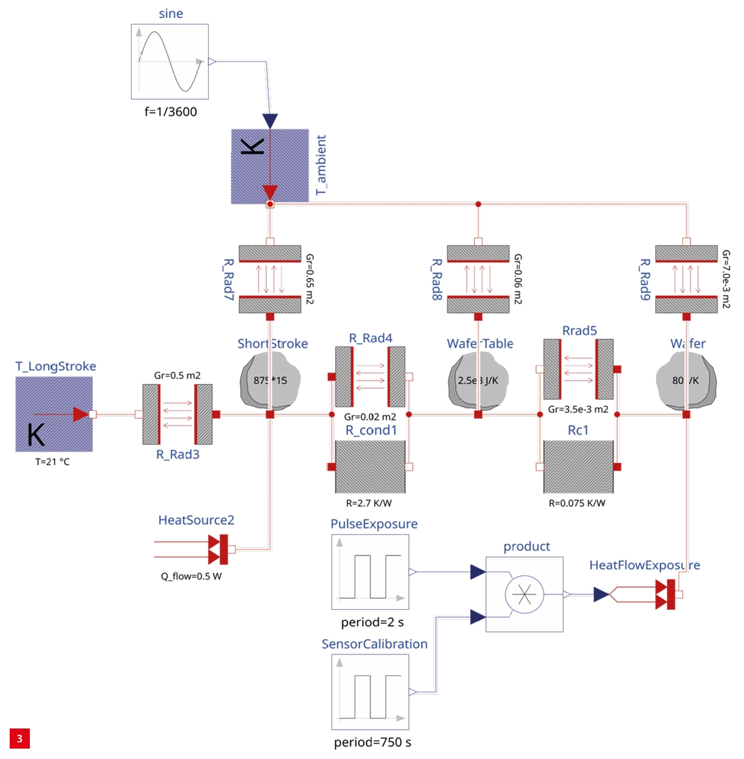
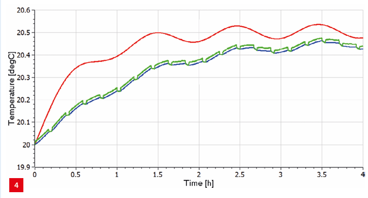
Through modelling of thermal systems, their thermal behaviour can be predicted and the effectiveness of thermal drift mitigation strategies can be evaluated. The lumped-element method (LEM) and the finite-element method (FEM) are often employed to model thermal systems, particularly in the early phases of engineering projects to evaluate the performance of concept designs and assess whether they match specified system requirements.

LEM modelling.

In the LEM method, a thermal system is divided into heat capacities, thermal couplings and heat or temperature sources. The essence of lumped capacitance is the assumption that the temperature of a component, represented by a single heat capacity, is spatially uniform at any instant during the transient process.

As an example of how thermal drift can compromise precision, a typical wafer stage was considered that consists of several components: base frame, balance mass, long stroke, short stroke, wafer table and the wafer (see Figure 1). The long-stroke position actuators are designed for extended range and high velocity. The short-stroke position actuators are designed for precision instead of distance and velocity. The wafer is a thin slice of crystalline silicon with a diameter of 300 mm and a thickness of approximately 0.7 mm. Wafers are the base material for the fabrication of microelectronic devices such as integrated circuits (ICs, microchips).

A wafer stage is required to position a wafer with nanometer-scale precision for successful photolithographic patterning of chip designs (see Figure 2). A wafer can go through the photolithographic cycle as many as 50 times. The pattern-to-pattern alignment between the layers deposited on the wafer (called the overlay) is crucial, since misalignment leads to short-circuits and connection failures in the integrated circuits.

Schematic overview of a typical wafer-stage positioning system
Schematic overview of a typical wafer-stage positioning system, with its components in a stacked configuration. The base frame surrounding the other parts is partially shown.
A wafer stage in operation
A wafer stage in operation: light is used to transfer an IC design pattern onto a wafer that is covered with a photosensitive material The wafer and reticle move in opposite directions during the exposure step. The wafer itself moves in a zig-zag pattern between exposures in order to transfer multiple IC design patterns onto a single wafer.

The thermal behaviour of the wafer stage can be assessed by constructing a LEM-model (see Figure 3) that includes the system components, heat/temperature sources and thermal interactions. The LEM-model in this example was constructed in OpenModelica [1], which is an open-source modelling and simulation environment based on the Modelica language. In this LEM-model of the wafer stage, it is assumed that the base frame is large and surrounds the other parts (effectively taking on the ambient temperature), and all other components are stacked and only have interaction with the component directly above or below it.

There is a heat source present in the short-stroke component, as well as a heat source resulting from the thermal dissipation of the photolithographic exposure of the wafer. This exposure is interrupted every 600 seconds for the remeasuring or recalibration of the wafer position. The ambient (or base-frame) temperature is not constant, but has a sinusoidal fluctuation of 0.2 °C with a period of 1 hour. It is assumed that the long-stroke component has a constant temperature of 21 °C. Furthermore, it is assumed that all components have an initial temperature of 20 °C.

Schematic overview of the LEM-model
Schematic overview of the LEM-model, including the system components, heat/temperature sources and thermal interactions.

After compilation of the LEM-model, a simulation with a total simulation time of four hours was performed, and the temperature of the system components during this time was plotted (see Figure 4). As can be observed from the graph, the temperature of all components increases as a result of the heat sources present in the system. The fluctuation in ambient temperature has the largest influence on the temperature of the short stroke. The temperatures of the wafer and wafer table are nearly identical, a result of the high thermal conductivity in the contact between these parts. The exposure-recalibration intervals are visible in the temperature profiles of these components. The system is approaching a thermal equilibrium after three hours of operation, but minor temperature fluctuations remain present.

Temperature curves as displayed in Figure 4 can be used to estimate the extent to which position accuracy of the wafer is compromised as a result of thermal drift. For example, if the temperature of the wafer increases with 0.4 °C, then a thermal expansion offset of approximately 160 nm from the centre of the wafer to the outer regions can be expected. A priori knowledge of this makes it possible to compensate for expected thermal expansion, and estimate appropriate remeasuring/recalibration intervals.

Temperature curve of the short stroke, wafer table and wafer
Temperature curve of the short stroke (red), wafer table (blue) and wafer (green) as calculated with the LEM-model

FEM modelling.

If temperature differences within components are not negligible, then a spatial discretisation method such as FEM needs to be used. As an example of how FEM modelling can be used to determine the influence of thermal drift on precision, the short stroke - also known as the mirror block of a wafer stage was considered (see Figure 5). In this example, the mirror block has two mirror planes that are used for position and orientation measurement through laser interferometry, and the mirror block is suspended using magnetic levitation with magnets attached to the bottom.

A wafer is clamped onto the wafer table, which is placed on a mirror block with two mirror planes on the sides of the block. The thermal centres of the wafer table and the mirror block are aligned and a statically determined mechanical coupling between the components is achieved through ball-groove interfaces. To position a wafer with nanometer precision, laser interferometers are used to measure the position and orientation of the mirror block (see Figure 6).

Any distortion of the flatness of the mirrors causes the position/orientation measurement of the mirror block to be compromised. The mirror block can be manufactured with extremely flat mirror planes; however, flatness distortion as a result of thermal expansion inside the mirror block cannot be completely avoided. A small amount of thermal dissipation is induced by eddy currents in the magnets attached to the mirror block (see Figure 5), which leads to a non-uniform temperature distribution in the mirror block and hence uneven thermal expansion that distorts the flatness of the mirror planes.

Short stroke of a wafer stage with two mirror edges
Short stroke (or mirror block) of a wafer stage with two mirror edges. (a) The triangular mechanical interface with the wafer table. (b) The magnets attached to the bottom.
Mirror-block assembly with two mirror planes
Mirror-block assembly with two mirror planes that are used for position and orientation measurement of the mirror black through laser interferometry

The level of flatness distortion and its impact on the accuracy of the position measurement was determined with a thermo-mechanical FEM analysis, using the finite-element-analysis software ANSYS Mechanical [2]. First, the temperature distribution in the mirror block needed to be determined by performing a thermal FEM analysis of the full mirror-block assembly. The analysis included the heat dissipation in the magnets, heat generated by the photolithographic exposure of the wafer and the radiation heat exchange between the components. The result of this analysis was a temperature distribution profile in the mirror block (see Figure 7), which was used as input for the mechanical FEM analysis, in which the deformation of the mirror block as a result of thermal expansion was calculated.

With the mirror block constrained at its thermal centre, the thermal expansion was calculated by imposing the temperature distribution from the thermal FEM on the mirror block, where the mirror block had an initial uniform temperature of 20 °C. The deformation profiles of one of the mirror planes is shown in Figure 8, displaying the out-of-plane deformation (normal to the mirror plane itself). It was necessary to extract this deformation profile from the FEM analysis results for further processing.

The average out-of-plane deformation of the mirror does not have a large influence on the magnitude of the measurement error, contrary to a rotation in the mirror plane, which can cause a much larger measurement error. By using the linear least-squares technique, a plane could be fitted to the deformation profile, from which the average out-of-plane deformation (x-offset) and rotations was extracted (see Figure 9): Rz = 0.122 µrad, Ry = 0.417 urad, x-offset = -5.265 µm. Additionally, also the maximum peak-to-valley distance (0.079 µm) and maximum local angle (4.032 µrad) were extracted from the dataset. These values were subsequently used to estimate the magnitude of the measurement error as a result of the thermal deformation of the mirror plane.

Non-uniform temperature distribution in the mirror block
Non-uniform temperature distribution in the mirror block as a result of thermal dissipation induced by eddy currents in the magnets attached to the bottom. The flatness of the mirror planes can be distorted because of uneven thermal expansion. Scale: 20.927 °C (blue) to 21.028 °C (red).
Deformation profile of one of the mirror planes
Deformation profile of one of the mirror planes, displaying the x-component of the deformation, which is oriented normal to the plane itself. Scale: -5.3233-10 m (blue) to -5.2186-10 m (red).
Least-squares plane fit of the mirror-plane x-component deformation profile
Least-squares plane fit (black grid) of the mirror-plane x-component deformation profile.

conclusion.

In precision engineering, the modelling of thermal systems provides essential insights into thermal behaviour and the effectiveness of thermal drift mitigation strategies. The lumped-element method (LEM) is often employed to model thermal behaviour of complex systems, as it allows for fast and relatively easy modelling of transient heating and cooling problems. If temperature differences within components are not negligible, then the use of spatial discretisation methods such as FEM is necessary, which is computationally much more expensive but can provide the level of detail that is required.

visit Demcon multiphysics
references

[1] Fritzson, P., et al., "The OpenModelica integrated environment for modeling, simulation, and model-based development, Modeling, Identification and Control, vol. 41 (4), pp. 241-295, 2022.

[2] Bhashyam, G.R, ANSYS mechanical - a powerful nonlinear simulation tool, Ansys, Inc, 1 (1), 39, 2002.

more cases & tech insights.

Demcon_hightech_measuring_surface_systemDemcon_hightech_measuring_surface_system

Measuring the nearly unmeasurable

Conventional spherical lenses suffer from spherical aberration. Therefore freeform – often aspherical – lenses have become popular in lithography, aerospace, astronomy and microscopy as well as in (smartphone) photography.

Read more
Demcon_hightech_inside_systemDemcon_hightech_inside_system

Glassfiber connection made easy

Lightning-fast internet via glass fiber – that’s what everyone wants. But one tricky point in roll-out is the manual connection of two fiber ends. That demands accuracy, takes time and requires skills. TE Connectivity developed a connector that lends itself to automatic processing by a so-called Light Plug Tool.

Read more
Demcon_hightech_full system_moduleDemcon_hightech_full system_module

Producing medical radio-isotopes with minimal nuclear waste

Radio-isotopes are widely used for medical diagnostics and treatment, predominantly in cancer care. The current production method has only a 2% yield of the isotope wanted. The rest is mostly nuclear waste. Demcon helps to produce it with minimal nuclear waste.

Read more
Demcon_hightech_dashboard_time-series_Demcon_hightech_dashboard_time-series_

Use cases in machine learning for time series

It is essential that the ventilator support is synchronized (in time) with the patient’s spontaneous breaths. A mismatch in this timing is referred to as Patient-Ventilator Asynchrony (PVA). To improve the patient’s comfort and recovery this PVA must be prevented. A key step in this process is the detection and classification of PVA.

Read more
Demcon high-tech systems logo diapositive
MarketsServicesExpertisenanoLEVQuantumShowcasesAbout usEventsNews

GET IN TOUCH

Demcon high-tech systems
+31 88 115 20 00

Send a message
Demcon high-tech systems is part of the Demcon group
Cookie policyPrivacy statement
© 2026 Demcon. All rights reserved.