
Semicon metrology & inspection
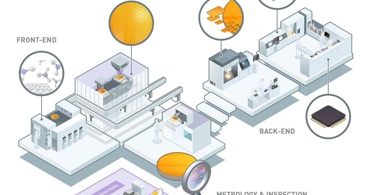
We support semicon metrology and inspection manufacturers with precision mechatronics, opto-mechanical systems, simulation, controls and system integration.
About
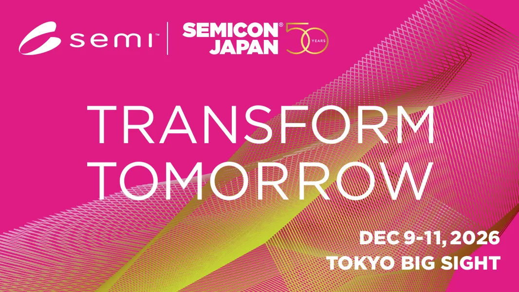
SEMICON Japan is one of the leading meeting places for the semiconductor supply chain in Asia, and in 2026 it celebrates its 50th edition. Device makers, OSATs, equipment manufacturers and suppliers come together in Tokyo to discuss the technologies that shape the industry. Two programs that run alongside the exhibition, the Advanced Packaging and Chiplet Summit and the Metrology & Inspection Summit, show where much of the attention lies this year.
One question guides our visit: what does the next generation of semiconductor devices demand from the equipment that manufactures and inspects them? Our multidisciplinary teams bring decades of experience in supporting semiconductor equipment makers with precision mechatronics and first-of-a-kind modules. Eric Meulenkamp, new business development manager, and Hiroshi Ishiwata, general manager of Demcon Japan K.K., represent Demcon high-tech systems in Tokyo and look forward to continuing these conversations in Japan.
The challenges we solve
Advanced packaging and hybrid bonding
We combine ever tighter alignment with the speed, cleanliness and reliability that chiplets and 2.5D/3D integration demand.
Metrology and inspection
We develop modules for optical, AFM, e-beam and X-ray systems that detect bond defects, warpage and alignment errors in advanced packages.
Precision positioning
We design fast, stable and clean stages, including the nanoLEV platform, for vacuum and magnetically sensitive machine environments.
Development partnership
We add specialized engineering expertise to our customers’ R&D teams, while product knowledge and ownership stay with the customer.
Connect with us at SEMICON Japan
We are looking forward to joining SEMICON Japan. Are you attending the event or working on challenges in advanced packaging, metrology or precision positioning? Send us a message to connect, or set up a meeting with Eric Meulenkamp and Hiroshi Ishiwata at the Holland High Tech Pavilion in West Hall 1 during the event.
Learn more about the event here.
Project highlight
In our hybrid bonding case, alignment of around 30 nm comes together with a throughput of 3,000 to 4,000 dies per hour. Meeting both targets in one system takes close collaboration between mechatronics, control, thermal design and cleanliness.
Read more about the project here:
We support semicon metrology and inspection manufacturers with precision mechatronics, opto-mechanical systems, simulation, controls and system integration.